Semiconductor Industry Application Solution (I) Thermal Desorption - 770 GC-MS & VOC/SVOC
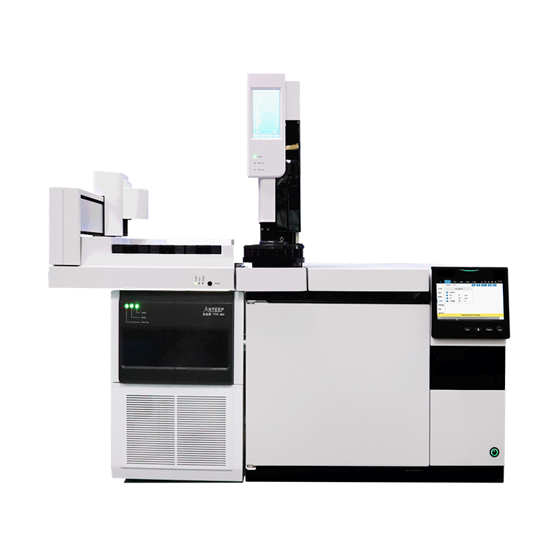
Thermal Desorption-7700 GC-MS System (Lab Offline): Specialized in medium-to-large molecule VOCs/SVOCs, photoresist pyrolysis products, encapsulant outgassing, and cleanroom AMC contamination. Solves complex organic pollution tracing challenges that online mass spectrometry cannot resolve.
Product Positioning and Roles
Thermal Desorption-7700 GC-MS System (Lab Offline)Specializes in large and medium-molecule VOCs/SVOCs, photoresist pyrolysis products, packaging outgassing, and cleanroom AMC contamination. Solves complex organic pollution source tracing challenges that online mass spectrometry cannot resolve.
II. Thermal Desorption-7700 GC-MS System for Semiconductor Applications
Core Product Features
High sensitivity and resolution, optimized for detecting large organic molecules in VOC/SVOC analysis to address gaps in online small-molecule mass spectrometry. Enables precise identification of trace complex organic pollutants, meeting the demands of high-precision failure analysis and material quality control in semiconductor manufacturing.
Segmented application scenarios
1. Semiconductor Consumables/Parts: Outgassing Traceability & Quality Control
For chamber seals, PEEK consumables, quartz components, sealants, and coatings, simulate high-temperature operating conditions via thermal desorption to analyze released organic contaminants. Select low-outgassing compliant materials, establish supplier incoming quality control standards, and control chamber organic contamination at the source.
2. Failure Analysis of Organic Contamination on Wafer/Cassette Surfaces
For bulk defective wafers, FOUPs, and wafer carriers, detect photoresist residues, cleaning solvent residues, and cleanroom AMC contaminants on surfaces to precisely identify root causes (consumables, chemicals, or environment) and rapidly resolve yield anomalies.
3. Reliability Analysis of Advanced Packaging Materials
Detect thermal degradation products of molding compounds, underfill adhesives, bonding adhesives, and encapsulation coatings. Identify high-risk SVOC impurities such as siloxanes, esters, and aromatics to evaluate the long-term stability of encapsulation materials and prevent post-encapsulation failures including delamination, corrosion, and electrical drift.
4. Periodic AMC molecular contamination inspection in cleanroom
Collect air samples from cleanrooms and around equipment using adsorption tubes to qualitatively and quantitatively detect volatile organic compounds at the ppb level. Verify cleanroom classifications, trace pollution sources, and ensure environmental cleanliness for advanced process manufacturing.
5. Purity verification of process chemical incoming materials
Detect volatile impurities and byproducts in photoresist, developer solutions, semiconductor cleaners, and other reagents. Verify incoming chemical quality to prevent wafer contamination and process window shifts caused by chemical volatiles.
III.Offline solution
1、 Offline Traceability (7700 GC-MS): Analyze complex macromolecular organic pollutants; precisely identify pollution sources and root causes of failure.
2、 Sample and retain: Upon exception trigger, quickly collect wafer and environmental adsorption samples.
3、Closed-loop process optimization: Reverse-mentor material replacement, process parameter adjustments, and equipment maintenance to eliminate recurring process defects.
4. Core Specifications and Selection Comparison Table (Commercial Concise Version)
Product Model | Core Positioning | Detect Substance | Deployment Method | Core Advantages |
Thermal Desorption-7700 GC-MS | Laboratory Organic Pollution Source Tracing Analysis | VOC/SVOC, photoresist pyrolysis products, encapsulant organic compounds, and AMC contaminants | Offline Lab Testing | Precise Qualitative Analysis, Root Cause Resolution for Complex Failures, and Material Quality Control |
5. Target Customer Segment
• Wafer fabrication companies: Logic, memory, and compound semiconductor (GaN/GaAs) production lines.
• Advanced Packaging Enterprise: Power Devices, MEMS, Optoelectronic Devices, SiP, and Fan-out High-end Production Lines
• Domestic semiconductor equipment manufacturers: etching, deposition, furnace annealing, and vacuum packaging system providers.
• Semiconductor Materials Manufacturer: Supplier of sealing consumables, encapsulation adhesives, process chemicals, and cleanroom consumables.
• Third-party testing agencies, semiconductor research institutes, and university laboratories.